
Mixed: MCU + AND gate + transistor (coexistence test)
Mixed: MCU + AND gate + transistor (coexistence test) is a runnable microcontroller simulation example on SensBench — open the wired circuit, inspect the code, and compile real firmware in your browser, no install needed. Last updated Aug 14, 2026.
FREE SIMULATOR EXAMPLE · INTERMEDIATE
Mixed: MCU + AND gate + transistor (coexistence test)
This example coexists an MCU, an AND gate, and a transistor driver on one canvas: pin 5 is a steady enable, pin 6 blinks at 1 Hz, and the load only runs when both agree. It is the pattern behind hardware interlocks — the gate adds a safety condition the code cannot violate.
| Board | Arduino Uno (ATmega328P) + logic / power circuit |
|---|---|
| Difficulty | intermediate |
| Category | circuits |
| Libraries | None — just the Arduino core |
| Runs in | Sensbench browser simulator — free, no account |
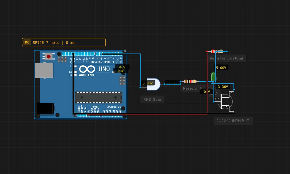
The exact circuit you get when you open this example — already wired, ready to run.
The sketch
// MCU + AND gate + transistor coexistence.
// pin 5 = steady enable, pin 6 = blink. AND(5,6) -> transistor -> motor LED.
void setup() { pinMode(5, OUTPUT); pinMode(6, OUTPUT); }
void loop() {
  digitalWrite(5, HIGH);                 // enable
  digitalWrite(6, (millis() / 500) & 1); // ~1 Hz blink
}
How it works
Pin 5 drives the steady enable line — always HIGH — and pin 6 carries a 1 Hz blink generated from millis(). The physical AND gate combines them: its output is HIGH only when both inputs are HIGH, so the transistor (and the load it drives) turns on only during the enable-and-blink overlap. The loop has no delays — the square wave comes from the counter.
The transistor at the gate’s output is the power stage: the gate’s logic-level output drives the base, and the transistor switches the actual load current. The sketch is deliberately minimal because the interesting parts — the gate and the driver — live in the circuit, not the code.
Before you build it for real
The AND gate’s inputs must be within its logic family’s valid levels — driving a 74HC gate from a 5 V MCU pin works, but a 3.3 V MCU output is marginal for HC gates and can cause the gate to read intermittently. The transistor base resistor is still required between the gate output and the base — the gate sources limited current, but the base-emitter junction clamps at 0.7 V and will pull whatever the gate allows. And the (millis() / 500) & 1 trick produces exactly 1 Hz only while millis() runs — any code that blocks the loop also freezes the blink, which is the trade-off for the no-state elegance.
Get the parts
Related examples
FAQ
Why route the MCU through an AND gate at all?
The AND gate adds a hardware safety condition: the load only receives power when BOTH inputs agree — the MCU’s enable signal AND the hardware signal. Even if the MCU’s code crashes and the pin stays high, the load stays off unless the other condition is also met. It is a cheap hardware interlock.
Why use millis() instead of delay() for the blink?
(millis() / 500) & 1 computes a 1 Hz square wave from the millisecond counter — no blocking, no state variables, and the enable pin stays driven the entire time. The loop runs at full speed, which matters when the MCU has other work to do.