
NAND SR Latch
NAND SR Latch is a runnable microcontroller simulation example on SensBench — open the wired circuit, inspect the code, and compile real firmware in your browser, no install needed. Last updated Aug 14, 2026.
FREE SIMULATOR EXAMPLE · INTERMEDIATE
NAND SR Latch
This example simulates a NAND SR latch on the Arduino Uno: two buttons set and reset a stored bit that survives releasing both — memory without a clock. The Serial Monitor prints a live truth table of the most fundamental memory element in digital electronics.
| Board | Arduino Uno (ATmega328P) + logic / power circuit |
|---|---|
| Difficulty | intermediate |
| Category | circuits |
| Libraries | None — just the Arduino core |
| Runs in | Sensbench browser simulator — free, no account |
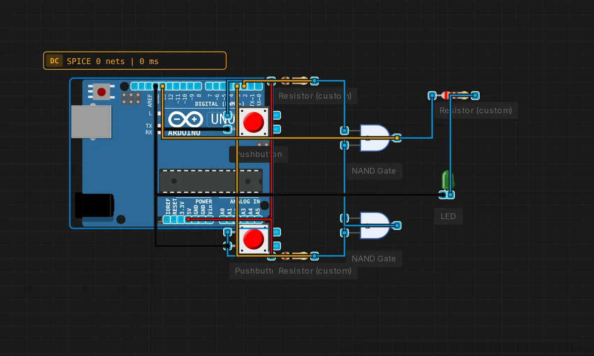
The exact circuit you get when you open this example — already wired, ready to run.
The sketch
// Software NAND SR latch simulation
bool q = false;
void setup() { Serial.begin(9600); pinMode(2,INPUT_PULLUP); pinMode(3,INPUT_PULLUP); pinMode(13,OUTPUT); }
void loop() {
  bool s = !digitalRead(2), r = !digitalRead(3);
  if(s && !r) q = true;
  if(r && !s) q = false;
  digitalWrite(13, q);
  Serial.print("S="); Serial.print(s); Serial.print(" R="); Serial.print(r);
  Serial.print(" Q="); Serial.println(q);
  delay(200);
}
How it works
Two buttons on pins 2 and 3 are the S (set) and R (reset) inputs, read with pull-ups and inverted. The loop implements the SR rules: S && !R sets the stored q to true, R && !S resets it to false, and anything else — both released or both pressed — holds the current state. Pin 13 mirrors q, and the serial line prints S, R and Q.
The 200 ms poll rate makes each press land cleanly in its own sample. The serial output is a live truth table: watch S=1 R=0 flip Q to 1, then release both buttons and see Q stay — the hold behavior that makes this a memory.
The forbidden state — both buttons pressed — is worth pressing deliberately: the NAND SR latch’s two outputs both go HIGH in that state, which breaks the Q = not-Q invariant. The software emulation keeps its single q unchanged, a small simplification the pitfall discusses.
Before you build it for real
The software version quietly sidesteps the latch’s forbidden state: on a real cross-coupled NAND pair, pressing both buttons drives both outputs HIGH, breaking the Q = not-Q invariant, and releasing both buttons simultaneously leaves the latch in a race — the stored value is unpredictable. Real SR latches also have a metastable window where the two feedback paths are still settling; sampling the output in that window reads garbage, which is why synchronous designs gate the latch with a clock. And the software latch here resets to false on every power-up — real hardware latches power up in a random state, which is why systems add a power-on reset pulse.
Get the parts
Related examples
FAQ
What does "memory without a clock" mean?
The SR latch stores a bit: set it, and it stays set until reset — no clock, no refresh, no CPU. Two cross-coupled NAND gates hold the state electrically. It is the fundamental memory element that every register in every processor is built from, shown at its most primitive.
Why does the sketch emulate the latch instead of wiring NAND gates?
This example teaches the latch’s behavior — the S=1/R=1 hold rule and the forbidden state — in software first, with the physical two-gate circuit available as the companion build. Once the software version’s truth table is understood, wiring the two cross-coupled NANDs makes the same table appear in hardware.